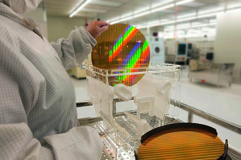
Openair-Plasma® in Semiconductor Manufacturing
Vacuum plasma has been used for many applications in the semiconductor industry. In the Openair-Plasma® process, a “reactive plasma zone” integrated into the plasma unit makes it possible to carry out continuous pretreatment during the ongoing production process. The potential-free Openair-Plasma® microfine cleaning system is ideal for the production of highly sensitive electrical components, replacing the vacuum chamber in the production of chip packaging in a much more efficient and cost-effective way. The method ensures a fast inline process and guarantees perfect uniformity regardless of your process and product.
FEATURES OF
OPENAIR-PLASMA®
in semiconductor manufacturing
- Selective area treatment possible
- High-speed treatment: Up to 1.5m/sec.
- Potential-free: < 1V, can also be used on sensitive electronics
- Cost-effective: Low investment and operating costs
- Flexible: Adaptable to all surfaces (flat or 3D)
- Environmentally friendly: No solvents thanks to the use of compressed air, VOC free technology
Video Semiconductor Manufacturing
- Dual lane concept
- Bar code scanning
- Control modules by PCU
- 100% yield and high-end product quality
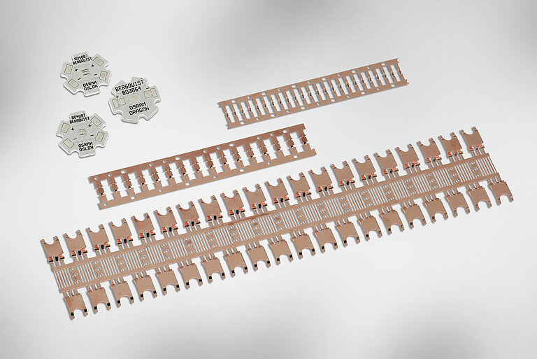
Leadframe and Packaging
Until now, unwanted oxide layers could only be removed prior to soldering or bonding processes by means of vacuum plasma chamber technology in a time-consuming and costly process. Openair-Plasma® microfine cleaning replaces the vacuum chamber in the production of chip packaging. A “reactive plasma zone” integrated into the plasma unit makes it possible to carry out continuous pretreatment during the ongoing production process.


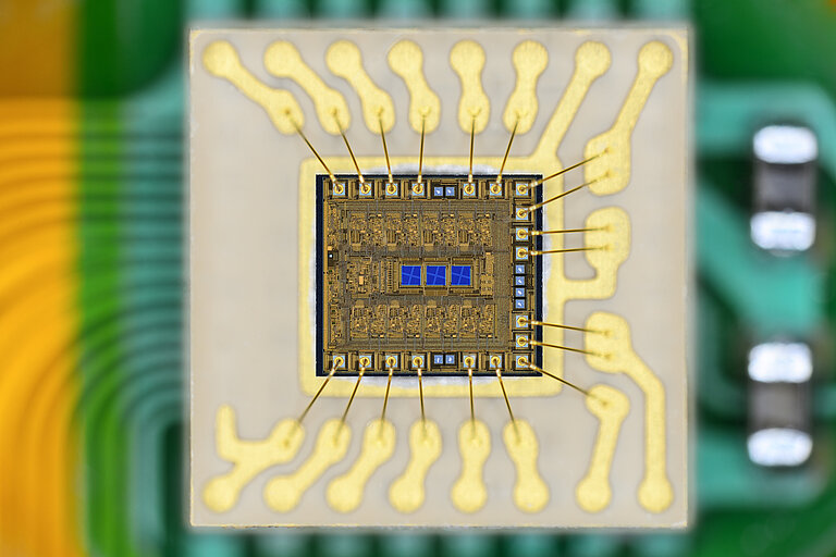
Die Bonding
Openair-Plasma® cleans surfaces, thus ensuring improved adhesion of die bond material and of soft solder. The strengthened bond between die and substrate that results from this in turn has a positive effect on heat dissipation. The high surface energy ensures that dies adhere without cavities. In addition, the higher surface energy achieved by the Openair-Plasma® process allows soft solder to be applied 50% faster. The Openair-Plasma® jets can also be integrated into existing die bonders.
Thermal Compress Bonding
In the thermal compress bonding process, dies can be placed and bonded to the pad by applying heat and pressure in a single step. As a result, the dies do not have to be subjected to a high temperature cycle in the reflow oven. This is especially advantageous for thin dies because they can deform when exposed to heat, thus resulting in failures. Moreover, the Openair-Plasma® process enables to treat the part selectively and avoids a full treatment of the part. This is a major advantage over methods commonly used in the past, which can only treat pads in their entirety. A plasma pre-treatment before applying flux ensures a perfect bond.


Wire Bonding
As standardized processes in electronics manufacturing, plasma processes ensure clean pads prior to wire bonding. However, a vacuum process entails challenges in terms of process duration and homogeneity. The Openair-Plasma® process can not only be integrated into the production line, but also yields consistent results in seconds regardless of batch size or process time.
Pre-Molding and Encapsulation
Here, the Openair-Plasma® process delivers higher substrate surface energy, thus providing a stronger bond between the components and encapsulation materials. The result is a more reliable and productive overall package.

Our next PlasmaTalks and Events
High-quality consumer cameras thanks to coordinated Openair-Plasma® surface treatment and special adhesives
Upcoming Exhibitions and Events
Get to know Plasma up close at our trade fairs and events!
NPE 2024
West Building Level 2 - Expo Hall, Booth W7479
Orange County Convention Center
Orlando, Florida
SMTconnect
Hall 4, booth 351
NürnbergMesse
Karl-Schönleben-Str.
Messeplatz 1
90471 Nuremberg
Germany
Advanced Engineering 2024
Booth P154
NEC Birmingham
North Ave, Marston Green
Birmingham