Openair-Plasma® in Electronics Components Manufacturing
Various electronic components are integrated into modern electronic devices, serving essential functions such as signal transmission, power delivery, and energy storage. These components are typically mounted on package substrates or printed circuit boards (PCBs), which are constructed by laminating multiple layers of conductive and insulating materials. This multilayer structure enables high-density integration, electrical reliability, and compact design — all of which are crucial for today’s advanced electronics.
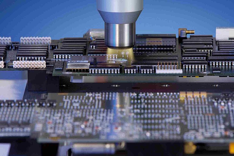
Abrasive Plasma – Alternative Procedure to Clean Drilled Holes (Desmearing) in Printed Circuit Boards

Drilled hole cleaning is an important step in printed circuit board processing prior to through-hole plating. Until now, this step was performed mainly in elaborate chemical or low-pressure plasma procedures that required interrupting the manufacturing process with separate chamber systems. In contrast, desmearing using the inline Openair-Plasma® process is done in atmospheric conditions, which simplifies and accelerates the relevant process and reduces costs as well.
Especially in conjunction with the use of industrial gases, the Openair-Plasma® process can form a strongly abrasive plasma that provides outstanding selectivity and high removal rates. The first installations of this new plasma technology are now in the preparatory stages.
Strong Adhesion of Multiple Layers using Openair-Plasma® Activation

Flexible printed circuit boards are now indispensible, especially in today’s mobile electronics. And flexible printed circuit boards are more and more frequently constructed of multiple layers due to the constantly increasing circuit component density. Firm adhesion is critical for trouble-free functioning of multiple-layer structures.
The adhesion between the individual layers is significantly improved with Openair-Plasma® activation. Since this often involves large-scale applications, systems with RD1010 plasma jets are used. The leading Japanese manufacturer of printed circuit board manufacturing equipment, Hitachi, offers this jet technology in its systems.
ADVANTAGES &
PROPERTIES
of Openair-Plasma® treatment for printed circuit boards:
- Potential-free surface treatment (e.g., super-fine printed circuit board cleaning)
- Makes new, more efficient process architectures feasible
- Eliminates whole production lines in the manufacturing process
- Makes it possible to selectively activate plasma in electronic components.