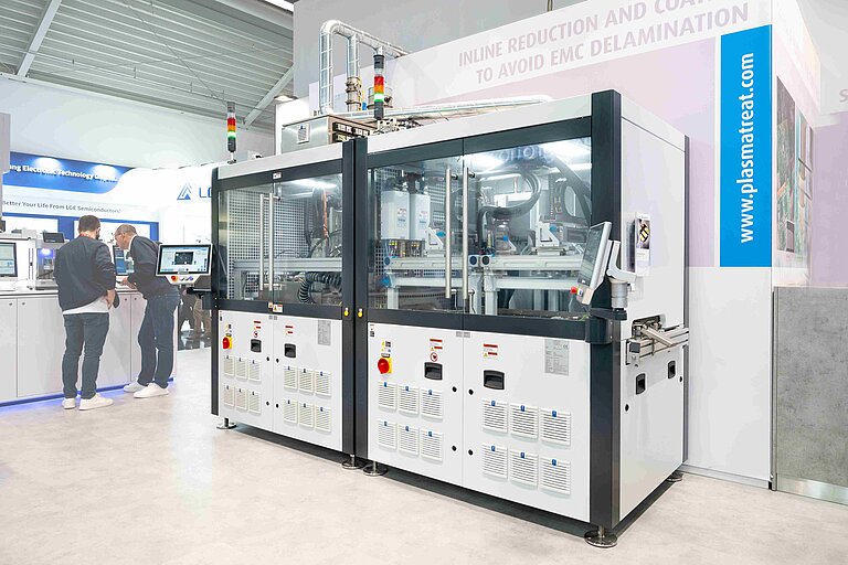
Improve Electronics Manufacturing Yield with Openair-Plasma®
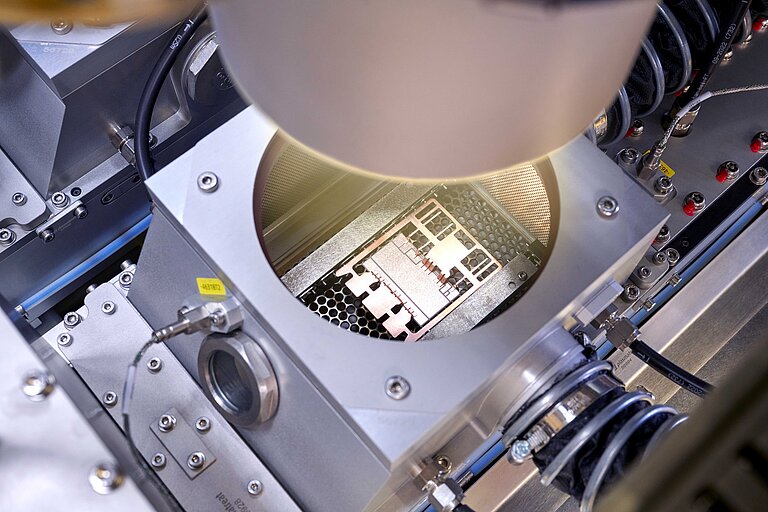
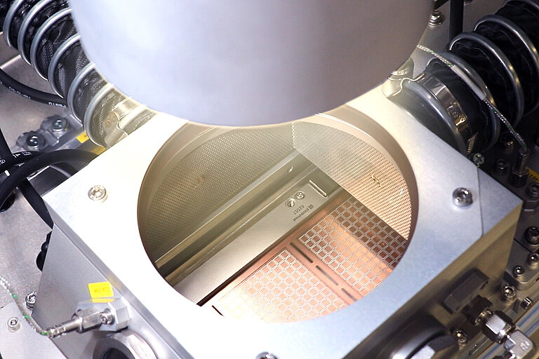
In electronics manufacturing, surface treatment is essential for ensuring strong adhesion between dissimilar materials, enhancing coating wettability, and maintaining long-term reliability. Plasmatreat’s Openair-Plasma® technology delivers precise, selective, and inline-capable plasma surface treatment under atmospheric pressure—without the use of vacuum chambers or chemical primers.
Variety of Applications


Physical surface modification using high-energy radicals
The smart alternative to wet chemistry
The Openair Plasma® process uses energetic oxygen and nitrogen radicals to modify surface molecules and create functional groups that improve adhesion.
For our customers in sensor and semiconductor production, this means more stable bonding processes, longer component life, and reduced scrap rates.
Consulting&
Resources
Discover how our Openair-Plasma® technology can enhance your processes. From the initial concept to successful implementation, we offer personalized, innovative, and sustainable support every step of the way.
The introduction of Openair-Plasma® was a milestone in the development of our sensor production.
Benefits of Openair-Plasma® technology
- Selective: switch on and off on the fly
- Super-fine cleaning (component cleaning) without damaging sensitive structures
- Targeted functionalization of surfaces for selective additional processing
- Environmentally friendly: no wet chemicals required
- Cost-effective: operates with oil-free compressed air
- In-line capability: no effect on process time because the plasma process takes less time than the conformal coating process
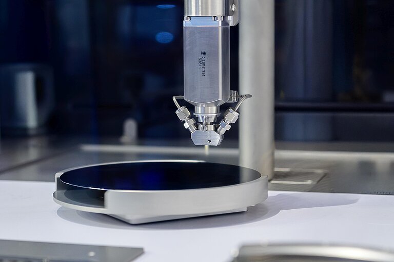
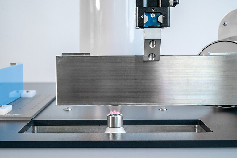
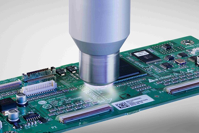
Openair-Plasma® process
Openair-Plasma® is used to modify surface characteristics so as to enhance the adhesion of materials (such as coatings) to the substrate (PCB). It removes all organic and silicone-based impurities. Oxygen in the form of hydroxyl and ketone groups are incorporated into non-polar surfaces to activate the surface. The result is high surface energy (over 72mN/m) and in most cases, complete wettability.