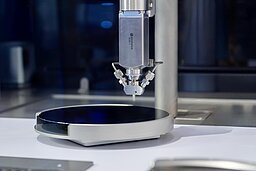
IMAPS: Advanced Plasma Jet and HydroPlasma Cleaning Technologies for Semiconductor Packaging

Plasmatreat USA, Inc., a subsidiary of Plasmatreat GmbH and a global leader in atmospheric pressure plasma systems and equipment, will showcase advanced solutions for particle-free, contactless, chemical-free, and inline-compatible surface pretreatment for semiconductor and electronics manufacturing at the IMAPS Device Packaging Conference, March 2–5, 2026, in Phoenix, Arizona.
As semiconductor devices continue to shrink while power densities increase, manufacturers face growing demands for surfaces that are exceptionally clean, oxide-free, and highly wettable to ensure reliable hybrid and chiplet bonding as well as wafer-level packaging. At the same time, flux residues, epoxy contamination, and oxide layers must be removed without chemicals while meeting stringent cleanroom requirements and maintaining consistent cycle times.
To address these challenges, Plasmatreat will present expanded plasma technologies designed to deliver low-particle, potential-free, dry surface preparation that integrates directly into inline production. These solutions enable both selective, localized treatment and uniform activation across large areas, resulting in stable interfaces, improved yields, and sustainable manufacturing processes without VOCs or aggressive chemical media.
Plasma Nozzle Technologies for Semiconductor Manufacturing
At IMAPS, Plasmatreat will highlight nozzle solutions based on Openair-Plasma technology that support hybrid bonding, wafer-level packaging, and advanced semiconductor assembly.
The PDW100 dielectric barrier discharge (DBD) nozzle is a flat atmospheric plasma solution with a treatment width of up to 100 mm, enabling uniform activation across large, sensitive substrates. The system removes organic residues and oxide layers without generating particles, supporting high process stability and repeatability.
The PFA10 plasma nozzle delivers low-particle, potential-free plasma treatment for highly precise, localized surface preparation. The nozzle effectively removes organic contaminants and oxides while activating metallic and polymer surfaces, creating optimal conditions for hybrid bonding and chiplet stacking.
“With the expansion of our plasma nozzle portfolio, we are enabling new levels of purity and process reliability in semiconductor manufacturing,” said Hardev Grewal, President and CEO of Plasmatreat North America. “The PFA10 and PDW100 provide uniform, contamination-free surface treatment that is essential for reliable electrical and mechanical connections, even in ISO Class 1 cleanroom environments.”
HydroPlasma Enables Advanced Residue and Oxide Removal
In addition to the nozzle technologies, Plasmatreat highlights HydroPlasma, an advanced cleaning process that combines the physical effects of Openair-Plasma with the chemical reactivity of ionized water molecules to remove stubborn organic and inorganic contamination.
During the HydroPlasma process, water is introduced into the plasma and ionized, creating highly reactive species that break down contaminants in a manner similar to detergent cleaning — but without chemical agents. The process is delivered through a precision jet, enabling targeted, non-abrasive cleaning of sensitive semiconductor components.
HydroPlasma is particularly effective for removing epoxy residues commonly left on metal surfaces after die attach, underfill, encapsulation, potting, and rework processes. It also removes naturally occurring metal oxides that can degrade adhesion, electrical performance, and downstream process yields. The result is oxide- and residue-free surfaces that improve bonding reliability and overall manufacturing consistency.
The technology provides efficient removal of organic and inorganic contamination, including heavy oil residues, while remaining environmentally friendly, VOC-free, and safe for use on metal, glass, and polymer surfaces.
Plasmatreat’s Openair-Plasma technology platform provides dry, chemical-free, and fully inline-capable surface treatment. The process reliably removes organic contaminants, silicones, and electrostatic dust while increasing surface energy to greater than 72 mN/m, supporting downstream processes such as die bonding, wire bonding, and underfill applications. Surface treatment is completed within seconds, delivers highly consistent results, and utilizes cost-effective process gases including compressed air or nitrogen.